GateMateTM FPGA Evaluation Board
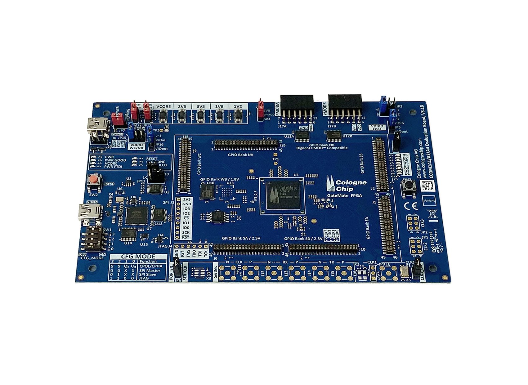
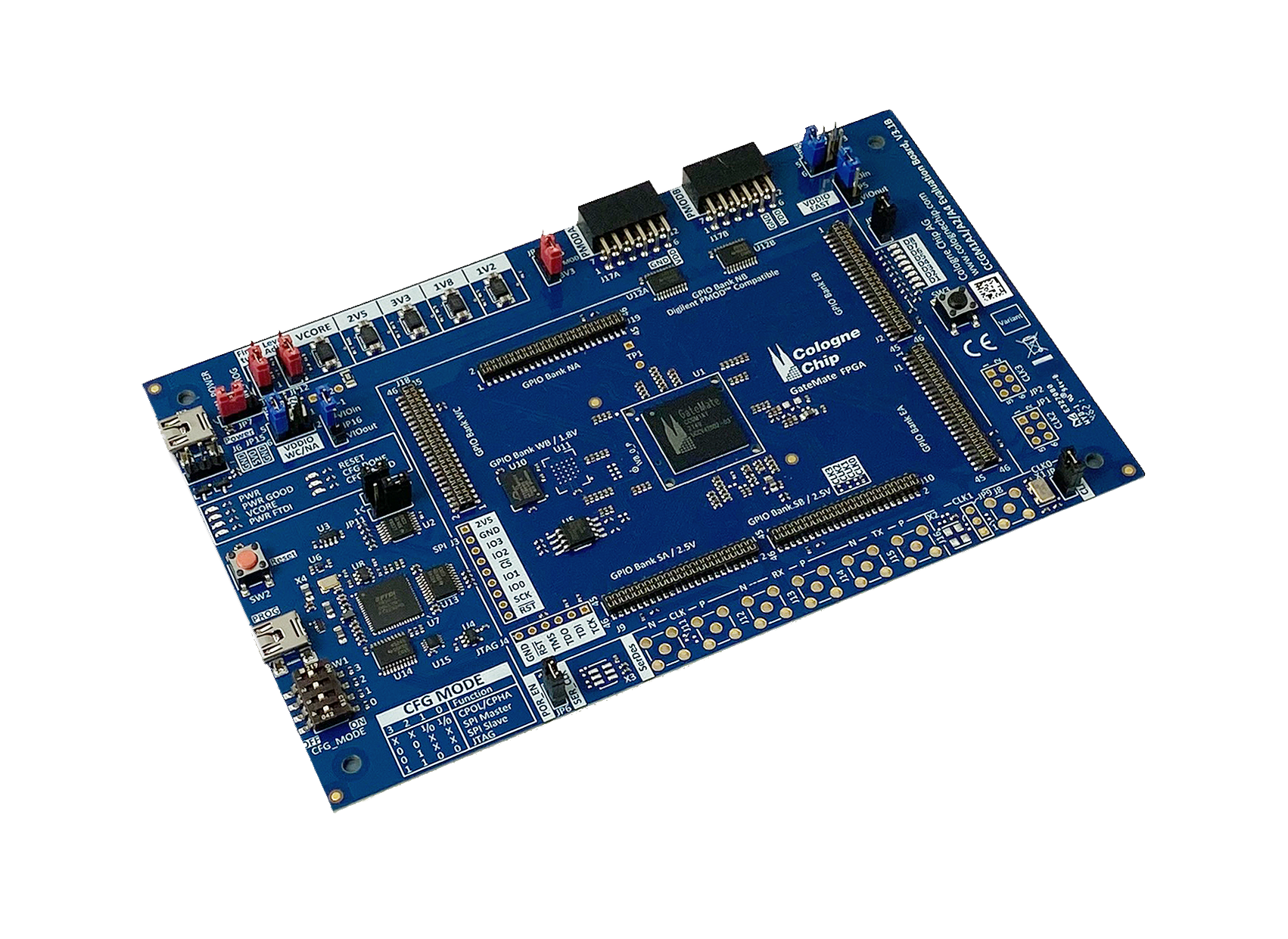
The GateMate™ FPGA Evaluation Board is a highly versatile and feature-rich development platform, specifically designed for the GateMate A1 and A2 FPGA devices. This ready-to-use board offers a convenient entry point for both, novice and experienced developers looking to create FPGA-based applications.
Equipped with an integrated on-board programmer, it provides seamless JTAG and SPI control via USB, simplifying the configuration process. The board supports six I/O banks, allowing for tailored user applications and maximum flexibility in design. Attaching additional hardware is straightforward, thanks to the Pmod connectors, which enable easy integration of a wide range of peripheral boards such as motor controllers, sensors, displays and more.
For high-speed data applications, the SerDes lanes are accessible through SMA connectors, providing robust support for demanding tasks that require fast serial data transfer. Whether you're developing complex systems or experimenting with FPGA capabilities, the GateMate™ FPGA Evaluation Board offers the ideal platform to accelerate your projects.
All Features of our GateMate TM FPGA Evaluation Board
GateMate A1 or A2 FPGA
Interfaces
|
Memory
Power
Dimensions
|
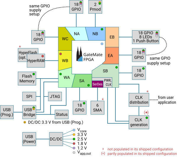
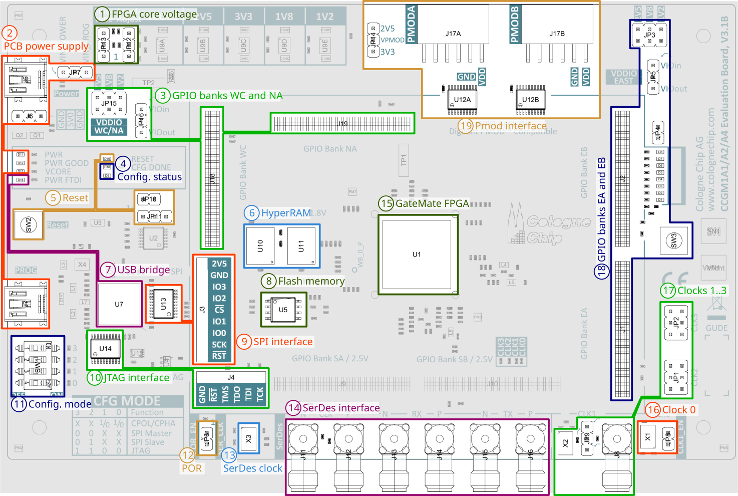
Block Diagram and Board Overview
The GateMate Evaluation Board features the new GateMate A1 and A2 FPGA. In order to offer the widest possible range of applications for your evaluation, the evaluation board offers all the minimum required peripheral components such as memory, clock, and access to a large number of interfaces and allows control over the core and IO voltages.


